 Emre Ceylan
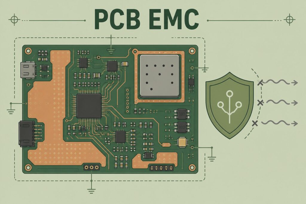
PCB EMC design is the engineering discipline that ensures an electronic board not only works, but remains stable despite ambient noise. In industrial environments, when motor drives, relay contacts and long cable runs share the same panel, weak grounding or unplanned layer usage distorts sensor readings, interrupts communication and causes frequent resets.
At Revan Technology, a significant share of the issues we encounter in embedded and industrial projects stems not from software bugs, but from poor electromagnetic compatibility (EMC) on the board. This article summarises what PCB EMC design means, typical field problems and practical solution approaches.

PCB EMC design — brief definition
PCB EMC design is the set of grounding, filtering, protection and placement rules applied on a printed circuit board to preserve signal integrity, limit external noise and prevent unwanted emissions from the device into its environment. The goal is predictable electromagnetic behaviour both inside the circuit and in the panel and cable environment.
This discipline is not limited to values measured in a test laboratory. When applied correctly, it prevents most field failures such as resets, incorrect sensor values and random communication dropouts already at the design stage.
Problem context
In industrial environments, EMC issues are often mistaken for “faulty boards” or “software bugs” and debugged for weeks. Yet the root cause is usually one of the following:
- Common-impedance grounding: High-current return paths and sensitive analogue lines are forced onto the same ground trace; ADC readings fluctuate.
- Long return path: Without a continuous reference under the signal trace, current cannot form a closed loop; an antenna effect occurs.
- Missing decoupling: Fast-switching digital ICs inject noise into the supply rail; neighbouring analogue circuits are affected.
- Insufficient protection and filtering: Without TVS, ferrite or RC/LC filters on I/O lines, external transients reach the processor directly.
This pattern is common in IoT and automation panels where a motor drive, GSM module and sensitive sensor share the same board. A circuit that works flawlessly on the prototype bench can behave like a different device once installed in a metal panel with long cables.
Technical analysis
Understanding PCB EMC design involves four fundamental layers: ground plan, power distribution, signal routing and protection.
1. Ground (GND) architecture
Star grounding or controlled split ground reduces cross-contamination between analogue and digital references. When analogue-digital separation is required, planes are joined at a single point; random bridges create loop currents.
2. Power and decoupling
Appropriate ceramic capacitors—and tantalum or electrolytic types where needed—are placed close to each IC supply pin. Low-ESR 100 nF together with 1–10 µF bulk capacitors limit supply rail noise at high frequency.
3. Signal routing
Critical traces are kept short with a continuous reference beneath them. Clock and high-speed data lines are kept away from analogue inputs. On differential lines, equal length and parallel go-return paths are maintained.
4. Protection and filtering
ESD and transient protection (TVS) on I/O ports, common-mode filters on industrial lines and ferrite beads or common-mode chokes where required. The connection between connector shell and board ground plays a critical role with shielded cables.
| Topic | Weak design | Strong EMC approach |
| Ground | Single plane, unplanned | Controlled partitioning + single tie point |
| Power | Remote decoupling | Close to pin, multi-layer capacitors |
| Cable exit | Direct to MCU | TVS + filter + shield continuity |
| Layer stack | 2-layer, wide traces | GND/power plane, controlled vias |
Field scenarios
In field tests, PCB EMC design gaps typically appear in these scenarios:
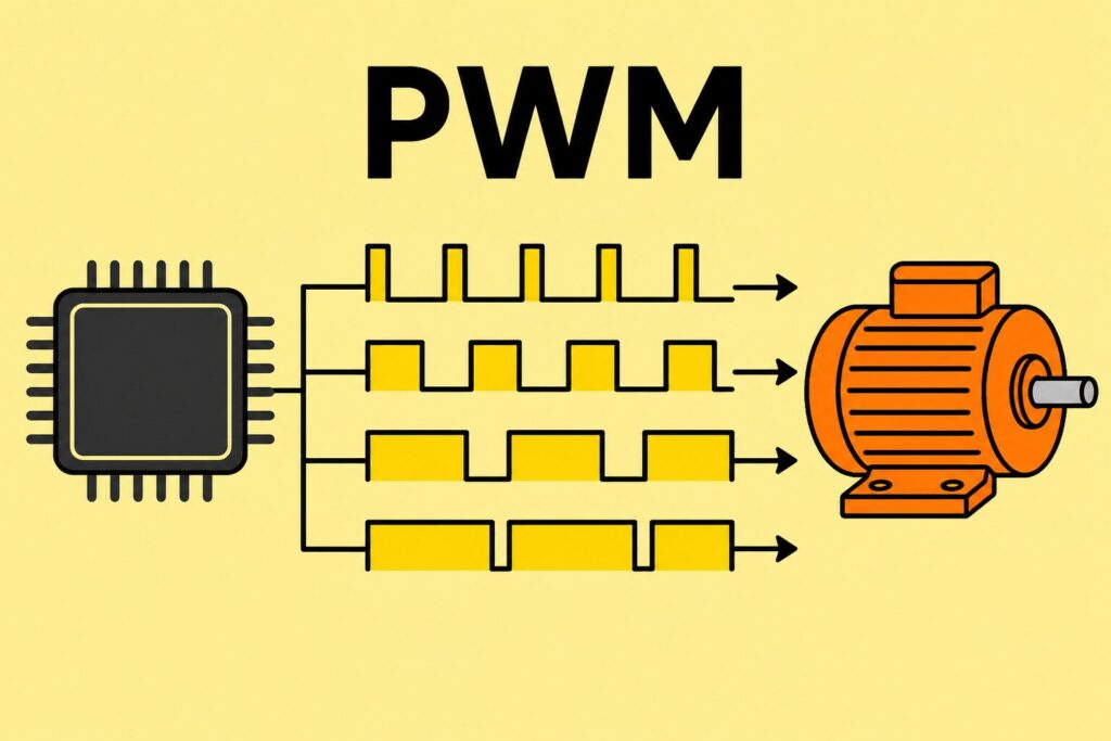
- ADC drift when motor starts: PWM drive return current couples onto the analogue ground and sensor line; temperature or pressure values jump momentarily.
- Reset when GSM module transmits: Sudden current draw causes brown-out due to insufficient bulk capacitance and weak supply path.
- Random errors on RS-485 or UART: Long cable shield is not bonded to panel ground or high-frequency reference is broken.
- CE/EMC test failure: Board passes at prototype stage; official measurement exceeds radiated or conducted emission limits.
The common thread in these scenarios is that the problem is not permanently solved by a software update; hardware revision or ground/filter changes are required.
Solution approaches
Practical strategies for robust PCB EMC design:
- Early layer plan: Ground partitioning, power tree and critical trace list are defined at schematic stage; layout is not patched afterwards.
- Reference plane priority: At least one full GND layer is allocated where possible; high-current paths are kept away from analogue areas.
- I/O protection template: Each external port is defined as a standard cell with TVS + series resistor + filter (RC or common-mode).
- Test points: Probe access is provided for ground, supply and critical signals; field debug time is shortened.
- Simulation and measurement: Pre-compliance scanning is performed on feasible projects; revision cost is reduced before production.
In Revan Engineering projects, these steps are balanced against board size and cost targets; focus follows risk analysis rather than unnecessary layers or excessive filtering.
Benefits
Concrete benefits of correct PCB EMC design:
- Fewer field failures: Reset, ghost sensor values and communication dropouts decrease.
- Shorter commissioning time: Weeks spent on panel “EMC patches” move to the design phase.
- Regulatory compliance: Approach to CE and industrial EMC requirements becomes easier.
- Service cost: Root cause is clear at hardware level; repeat field visits decrease.
- Product reputation: A stable device increases customer confidence and reference potential.
Sector observation / experience
The pattern we observe in industrial automation and IoT projects is this: EMC issues usually become visible as the product matures—as cables lengthen, panel density increases and serial production accelerates. Saying “it works” on the prototype bench does not provide the same confidence under field conditions.
In successful projects, PCB EMC design is not a detail the layout engineer adds later; it is a requirement defined from the start together with schematic, BOM and test plan. Especially on boards with motor drives, wireless communication and precision measurement, this discipline is one of the most effective investments for reducing total project cost.
Conclusion
PCB EMC design is the quiet but critical backbone of industrial boards. When grounding, decoupling, filtering and controlled placement come together, the device runs predictably not only in the laboratory but also in noisy field environments. Placing EMC at the start of embedded and industrial projects prevents costly field interventions later.
🔗 Get in touch with us:
Phone/WhatsApp: +41 76 212 8248
📧 E-Mail: info@revantechnology.ch
For detailed information about our services in electronics development & PCB design:
Revan Technology – Your partner for professional electronics and PCB development