 Emre Ceylan
The SPI protocol is one of the most widely used synchronous serial interfaces for fast data exchange with peripherals such as flash memory, ADCs, sensors, display drivers, and RF modules on microcontroller-based boards. Its single-master, multi-slave architecture, simple bus structure, and support for high clock frequencies make it a preferred choice in embedded projects.
However, if the four lines are not defined correctly, the wrong mode is selected, or routing on the PCB runs close to noisy power paths, a circuit that appears stable in the lab can become prone to periodic communication dropouts and data corruption in the field.

SPI protocol — brief definition
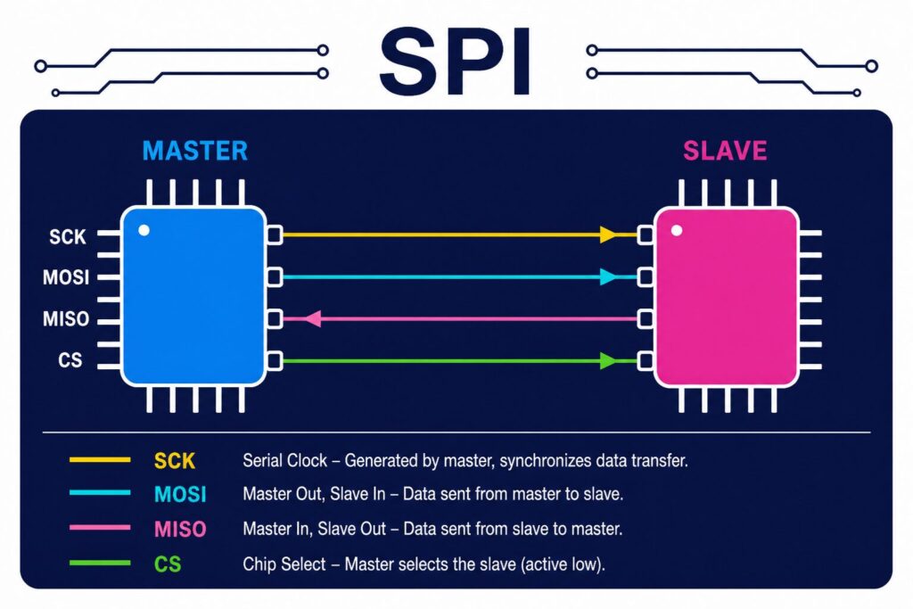
Serial Peripheral Interface (SPI) is a full-duplex protocol in which the master device generates the clock signal (SCK) and data is transferred synchronously over the MOSI (Master Out Slave In) and MISO (Master In Slave Out) lines. A separate Chip Select (CS, SS) line is used for each slave device; only the selected slave participates in data exchange while CS is active.
Data is typically transferred in 8- or 16-bit frames. Modes 0–3 define combinations of CPOL (clock polarity) and CPHA (clock phase); master and slave must use the same mode. SPI peripherals on most MCUs support DMA, reducing CPU load and enabling sustained high data rates.
Problem context
In embedded design, SPI is often seen as "fast and simple"; this perception leads to overlooking the physical-layer limits of the protocol. Long flat cables, connector transitions, shared CS lines, or incorrect pull-up/pull-down values degrade signal integrity. At clock frequencies above 10 MHz, rise times, reflections, and crosstalk become noticeable.
When multiple slaves share the same bus, only one CS line should be active at a time. If CS is asserted late or deasserted early, the slave may read the first or last bit incorrectly. Some flash and ADC ICs may not be ready for a certain period after power-up; SPI access during this window causes silent errors.
Technical analysis
The key design parameters are:
- Clock frequency: The slave datasheet maximum SCK, cable/PCB delay, and setup/hold times must be evaluated together. Testing should be done at the lowest temperature and highest supply tolerance.
- Mode selection (CPOL/CPHA): Master and slave must use the same mode; different modes produce bit shifts and inconsistent reads.
- CS management: Independent GPIO or a decoder (e.g. 74HC138) can be used per slave. CS transitions should occur while SCK is idle.
- Pull-up/pull-down: Appropriate resistors must be defined on open-drain or tri-state MISO lines; otherwise a floating pin reads incorrect bits.
- Power and ground: SPI lines should be kept short and straight; placed away from analog and power-switching paths.
- DMA and buffering: For high-speed flash read/write, double buffering and DMA reduce CPU intervention.
For example, on a display driver with 25 MHz SCK and a 20 cm flat cable, series resistors (22–47 Ω) and source-side termination can reduce rising-edge ringing. MOSI, SCK, and CS should be examined together on an oscilloscope; setup/hold violations should be detected before lowering the frequency.
Field scenarios
- Mode mismatch: If a newly installed sensor module uses different CPOL/CPHA, read values appear constant or random; the issue is mode matching, not the software driver.
- CS conflict: Selecting two slaves at once causes bus contention on MISO and corrupts the master input.
- Access during power-up: Sending an SPI command before flash or an RF module is ready yields no response; watchdog or reset cycles may trigger.
- Long cable and EMI: SPI lines near a motor drive are corrupted by impulse noise; communication may appear to work only when the motor is stopped.
- Wrong bit order (MSB/LSB): If the driver is MSB-first and the slave expects LSB-first, values are read reversed; calibration tables become meaningless.
Solution approaches
First, read maximum SCK, mode, CS polarity, and power-up time from the slave datasheet; each line should be clearly labeled on the schematic. On the PCB, SCK and MOSI/MISO traces should be equal length and as short as possible; a continuous ground plane under the reference is preferred.
In software, the SPI init routine should take mode and frequency from a central configuration table. CS control should run in a critical section; incomplete transfers during interrupts or RTOS context switches must be finished. On error, timeout, CRC, or retry mechanisms should apply; silent failure is not acceptable.
In production test, loopback (MISO–MOSI short) and known-pattern read/write can be verified automatically. If cable length or connector type changes in field revisions, SCK frequency should be rescaled.
Benefits
- Low latency for flash, display, and sensor updates thanks to high data transfer speed
- Low pin-count cost due to simple bus structure (faster than I²C, more pins)
- CPU freed for other tasks through DMA support
- Flexible adjustment of mode and frequency in software
- Fast verification via oscilloscope and loopback for test and diagnosis
- Stable communication in industrial noise environments with correct PCB layout
These benefits improve operational efficiency especially in scenarios such as HMI updates, firmware loading, and high sampling-rate ADC reads.
Industry observation / experience
In the field, most SPI-related faults stem from assuming the protocol "works by itself": mode matching is not checked, CS timing is not measured, and frequency is not reduced when the cable gets longer. In Revan Technology projects, the SPI bus is documented in the same package as power design and embedded software, so field assembly and software updates rely on the same reference schematic.
On multi-slave boards, CS decoders and series resistor selection provide repeatable behavior in serial production. Oscilloscope captures and frequency margin serve as concrete evidence in design revisions.
Result
The SPI protocol offers fast and flexible data transfer in embedded systems; reliable results require mode matching, CS management, clock frequency limits, PCB layout, and software timeouts to be designed together. Validating hardware and software against the same error budget prevents communication dropouts and data corruption in the field at an early stage.
🔗 Get in touch with us:
Phone/WhatsApp: +41 76 212 8248
📧 E-Mail: info@revantechnology.ch
For detailed information about our services in electronics development & PCB design:
Revan Technology – Your partner for professional electronics and PCB development