 Emre Ceylan
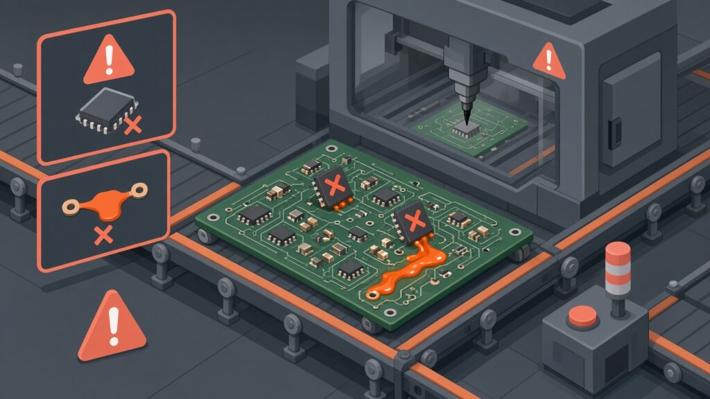
Boards that are perfect as a prototype but catastrophic in mass production are among the most common surprises when moving from sample validation to the assembly line. Firmware stable on the bench, a design that looks fine on hand-soldered or small-batch PCBA, produces a different failure profile on automatic pick-and-place, reflow profiling, and panel depaneling.
The four cases below are compiled from electronics board manufacturing and PCB design revision notes at Revan Engineering; no customer names, machine brands, or factory identities. The common theme: DFM steps skipped in prototyping turn into line cost in serial production.

Perfect as a prototype catastrophic in mass production — what does it mean?
This phrase means functional validation (bring-up, software test, short field trial) does not guarantee serial assembly quality. In prototyping, a single board, a wide-tolerance stencil, or hand assembly is used; component rotation, pad paste, panel edge clearance, and missing test points can go unnoticed. In mass production, the same Gerber file repeated thousands of times on an automatic line makes tombstoning, bridging, insufficient solder, and depanel cracks statistically visible.
“Catastrophic” here usually does not mean fire; it means high scrap rate, ICT/FCT rejects, delayed shipment, and urgent ECO cost. Even if the board works electrically, AOI/X-ray rejects or test fixture contact failures stop the production line.
Problem context
The customer approves the prototype board and places a serial order. The first batch of 500 units arrives on panels; after reflow, 8–12% visual solder defects are reported, ICT cannot reach the power rail test point, or SMD capacitors pop off during depaneling. The design team says “it worked in prototype”; the assembly line says “same Gerber.” The gap in between is DFM and process window difference.
Because prototype budget is kept low, panelization, fiducials, test pads, and stencil revision are deferred. When the serial quote arrives, the factory sends a DFM report; but if the order date is tight, revision does not fit. Result: either scrap is accepted or urgent spin causes delay.
Technical analysis — four real cases
Case 1 — Tombstoning (0402 resistor, reflow): In prototype, hand solder or wide paste windows kept 0402 resistors upright; in serial reflow they tombstoned. Pad sizes equal, thermal imbalance; paste on the smaller pad melted first, component stood on one end. AOI 6% reject. Fix: pad matching, thermal relief, stencil aperture reduced to 65%, component rotation aligned to reflow direction.
Case 2 — Panel edge and pick-and-place collision: Large QFP was placed 0.3 mm from the corner; no issue on single-card prototype order. On panel, mouse bite and edge clearance made nozzle access insufficient; pick-and-place offset and missing components. Fix: critical ICs moved toward panel center, panel outline revised, fiducials added on panel edge.
Case 3 — Via-in-pad and closed vias: Via-in-pad used on power stage; prototype fab filled vias by hand. Serial fab required closed vias and planarization; pads without filled vias showed voids and cold joints. Fix: thermal pad + separate via instead of via-in-pad, or closed via + backdrill spec added to layout.
Case 4 — Test point and FCT fixture: In prototype, measurement was done on random vias with a probe. Serial ICT fixture required 1.0 mm test pads and minimum edge distance; no pad on power rail. FCT jig pogo pins heated at high current, contact resistance fluctuated. Fix: test pad added for every critical net, jig hole map matched layout, high-current line got separate probe point.
Field scenarios
- IoT gateway, 1000 units/month: Prototype OK, serial batch 10% AOI reject; shipment delayed two weeks
- Motor driver board: Via-in-pad void under power MOSFET; returned field units with thermal shutdown
- Sensor interface board: Micro crack in flex zone during panel depanel; failure under field vibration
- Retrofit control board: Old form factor kept; component density exceeded pick-and-place limit, manual completion cost rose
- Urgent ECO: BOM swap only, stencil unchanged; pad mismatch caused bridging
Solution approaches
Before going serial, running a pilot panel (50–100 units) with the same factory and stencil profile shows the process window gap between prototype and serial early. Layout is updated to serial DRC set for panelization, fiducials, depanel path, and test pads. Stencil aperture is simulated per pad; 0402/0603 groups at tombstone risk get rotation and thermal pad revision.
In the Revan process, target assembly line and test strategy (ICT/FCT/flying probe) are asked at PCB design stage; on electronics board manufacturing side, factory DFM report is closed with layout revision. Assembly and test jig preparation run parallel to firmware bring-up — a “working prototype” alone is not a serial approval certificate.
Gains
When boards perfect as a prototype but failing in mass production are fixed with early DFM revision, scrap rate drops to single-digit percentages, ICT/FCT setup time shortens, urgent ECO and stencil change cost decreases. Measurable target: AOI reject rate below factory target on first serial batch, ICT yield 95%+, depanel without damage.
When design team and assembly line share a common DFM checklist (panel, paste, test, depanel), the “it worked in prototype” debate closes on data.
Sector observation / experience
A design passed with “fast and cheap” stencil on prototype order often causes the same pad geometry to fail when serial quote is taken. “We’ll add test points later” raises fixture cost and first-month scrap. Bare board order without panel planning creates mechanical stress on boards carrying SMD load during depanel.
DFM is not just factory CAM file check; pick-and-place, reflow, AOI, and test access must be considered together. Hand-reworked solder on sample board cannot be repeated by automation on the serial line. IPC assembly process guides (e.g. IPC-A-610) define accept/reject criteria that differ from bench bring-up judgment.
Sonuç
Boards perfect as a prototype but catastrophic in mass production arise from mixing functional validation with process fit. The four cases share tombstoning, panel edge placement, via-in-pad process difference, and missing test pads. Pilot panel, factory DFM revision, and test jig planning before serial conversion turn bench success into assembly line quality.
🔗 Get in touch with us:
Phone/WhatsApp: +41 76 212 8248
📧 E-Mail: info@revantechnology.ch
For detailed information about our services in electronics development & PCB design:
Revan Technology – Your partner for professional electronics and PCB development