 Veysi Filiz
ADC sampling and resolution are the key parameters for reliably reading analog sensor signals such as temperature, pressure, current or voltage on a microcontroller. On industrial embedded boards, saying “we have a 12-bit ADC” is not enough; if sampling rate, reference voltage, input impedance and anti-aliasing filter are not considered together, field readings fluctuate, thresholds trip falsely or calibration drifts again and again.
In Revan Technology projects, the ADC layer is planned as early as sensor selection, because analog errors that cannot be fixed in software become expensive on the production line.
ADC sampling and resolution — definition
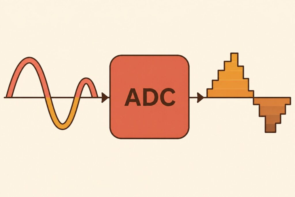
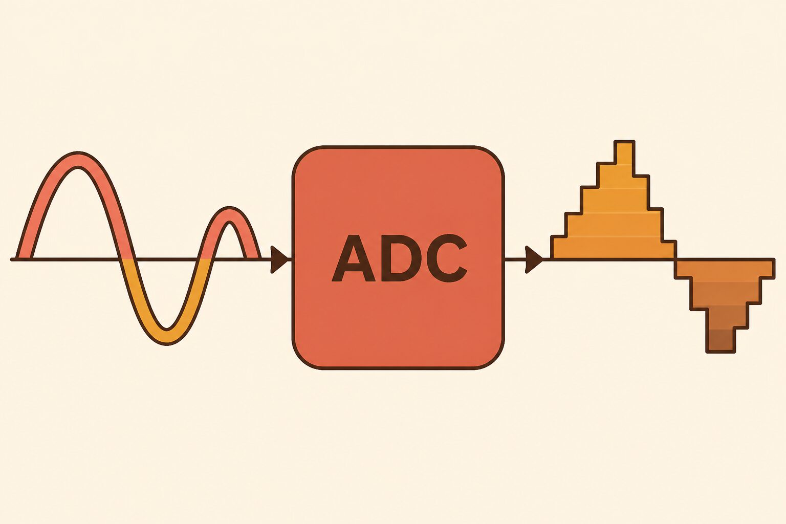
An Analog-to-Digital Converter (ADC) samples a continuous analog voltage at set intervals and converts it to a digital value. Sampling is how many measurements per second (Hz or kSPS); resolution is how many bits the ADC uses to distinguish levels. A 12-bit ADC theoretically represents voltage in 4096 steps (2¹²); with a 3.3 V reference, one LSB is about 0.8 mV.
Acquisition time, channel switching time and conversion time together define the period. In multi-channel scan mode, each channel’s effective sampling rate is divided by the number of channels. External reference (Vref), internal reference or ratiometric measurement (sensor supply = reference) directly affects accuracy.
Problem context
A sensor that reads stably in the lab may behave differently when mounted in a field panel or machine enclosure. Shortcomings in the ADC layer are often blamed on software; the root cause is on the analog side. Common problems:
- Aliasing: Violation of the Nyquist rule; high-frequency noise appears as false low-frequency ripple below the sampling rate.
- Reference noise: Switch-mode power supplies, motor drives or relay switching couple into the Vref line; all ADC channels jitter at once.
- High source impedance: If sensor output impedance is high, the sample-and-hold capacitor does not fully charge before conversion; error increases when switching channels.
- Resolution illusion: A “12-bit” label when ENOB (Effective Number of Bits) is around 10 bits does not meet expected distinguishability.
- Common-mode voltage: Long sensor cables and ground potential differences couple into low-voltage ADC inputs; differential or isolated measurement may be required.
So the “read ADC and average” approach hides the problem when sampling rate and filtering are wrong; it does not provide a lasting fix.
Technical analysis
Nyquist and anti-aliasing. The signal bandwidth to be measured must stay below f_s/2. For example, 50 Hz vibration analysis needs at least 100 Hz sampling; in practice 500 Hz–1 kHz is preferred. An analog low-pass filter (RC or active) before the ADC limits high-frequency content.
Resolution and LSB calculation. Voltage step: LSB = Vref / 2^n. If shunt drop for current measurement is 0–100 mV, 12 bits with 3.3 V reference uses only a small part of the card’s dynamic range; amplification (op-amp) or a lower reference may be needed.
Reference and calibration. Internal reference suits rapid prototyping; on industrial boards an external precision reference (e.g. 2.048 V or 4.096 V) reduces temperature drift. Offset and gain calibration can be applied in software at factory or field service; analog design must leave enough margin.
Channel scan and DMA. On multi-sensor cards, ADC + DMA + timer trigger reduces CPU load and gives evenly spaced sampling. Interrupt-based reads can cause jitter under heavy load.
Differential and isolated measurement. In 4–20 mA loops or environments with high common-mode voltage, differential ADC inputs or isolated amplifiers (e.g. AMC1301) are preferred. Single-ended reads suit short-distance, low-noise on-board measurement.
Field scenarios
Temperature and pressure monitoring. For slow signals, 1–10 Hz sampling may be enough; but if compressor or pump vibration couples onto the same line, filter and averaging window must be designed together.
Current shunt measurement. Millivolt-level drop on a motor line is exposed to microvolt noise in high EMI environments. Differential amplifier, short PCB traces and RC filter before the ADC are applied together.
Potentiometer / analog setpoint. When an operator knob is read at 10-bit resolution, mechanical vibration swings at the LSB limit; software hysteresis or median filter may be needed.
Multi-channel data logging. When ten channels are scanned simultaneously on an energy analyser or machine test card, effective per-channel sampling rate is calculated; one slow channel can delay the whole scan.
Solution approaches
In Revan Technology board designs, ADC sampling and resolution are clarified in these steps:
1. Sensor profile: Signal range, source impedance, expected bandwidth and ambient noise are defined.
2. ADC selection: Bit count, channel count, differential support, internal PGA and maximum sampling rate are set.
3. Analog front end: Protection, filter, amplification and reference circuit are calculated in the schematic.
4. Sampling plan: Timer/DMA period, channel order and anti-aliasing cutoff frequency are chosen consistently.
5. Calibration: Offset/gain, temperature coefficient and unit conversion test procedure are written.
6. Verification: Known reference source, noise injection and corner temperature tests are run.
The prototype decision “internal reference is enough” often forces revision in series production when temperature and supply tolerance widen; margin is therefore built in from the start.
Benefits
- A repeatable, traceable link between sensor data and the actual physical quantity is established.
- False threshold trips and nuisance alarms decrease.
- Calibration time shortens; field service cost drops.
- Consistent per-channel sampling timestamps on multi-channel systems.
- The measurement layer becomes more robust against EMI and supply ripple.
Industry observation / experience
In industrial projects, most second-wave ADC issues come from trusting the “12-bit” figure on the datasheet. Real ENOB can fall below 10 bits with reference noise and PCB layout; the operator UI may promise “0.1 °C accuracy” while hardware cannot support it.
Also, when one channel has a long cable and another a short connection on a multi-channel card, channel switching errors appear during scan; acquisition time or front-end buffer must be adjusted accordingly. Revan field records show cases where pump frequency appeared as “measured pressure ripple” on pressure lines without anti-aliasing filter — proving analog filter cost is cheaper than software filtering alone.
Conclusion
ADC sampling and resolution are the critical bridge that carries the analog world into digital on embedded boards. With correct sampling rate, sufficient effective bit count, clean reference and proper analog front end, sensor readings become reliable. On a new measurement card or IoT node design, treating the ADC as an upfront engineering input rather than a “we’ll handle it later” block shortens field commissioning and warranty processes.
🔗 Get in touch with us:
Phone/WhatsApp: +41 76 212 8248
📧 E-Mail: info@revantechnology.ch
For detailed information about our services in electronics development & PCB design:
Revan Technology – Your partner for professional electronics and PCB development