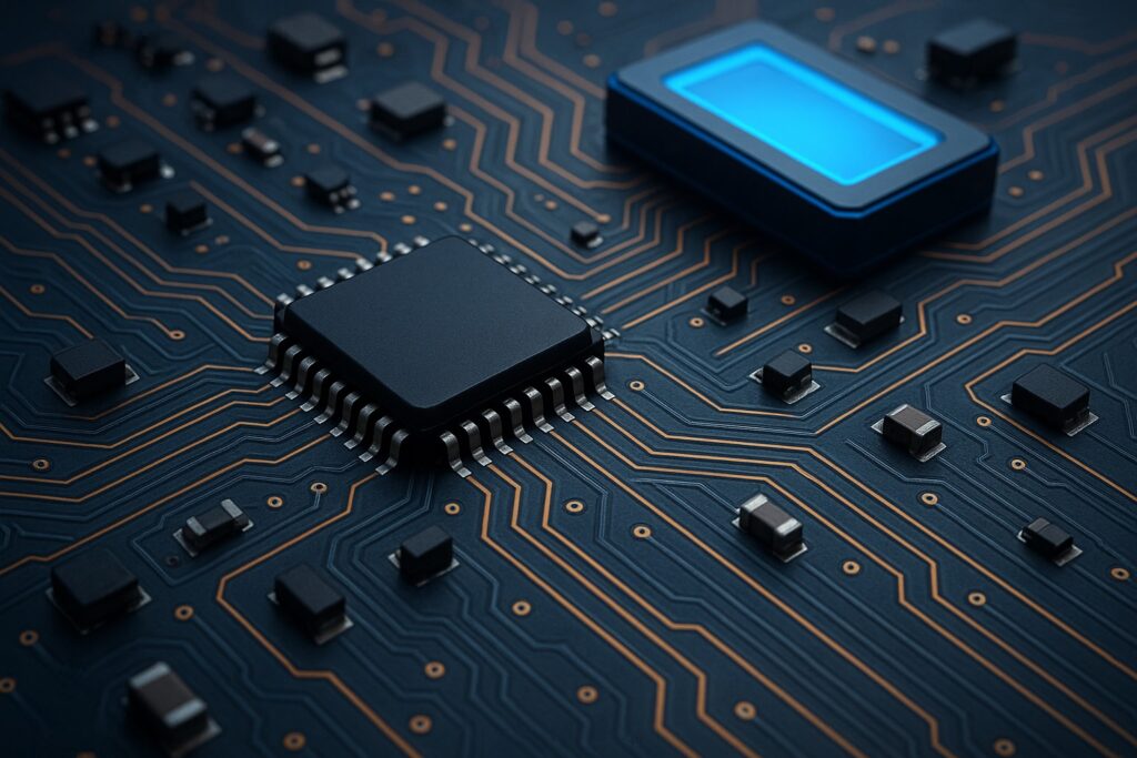
Revan Technology has extensive expertise in developing printed circuit boards (PCB design) for projects of any size and complexity.
For industrial projects, we design multilayer, high-durability control boards suitable for harsh field conditions. For prototypes and small-scale production, we offer compact, cost-effective, and quickly manufacturable board solutions.
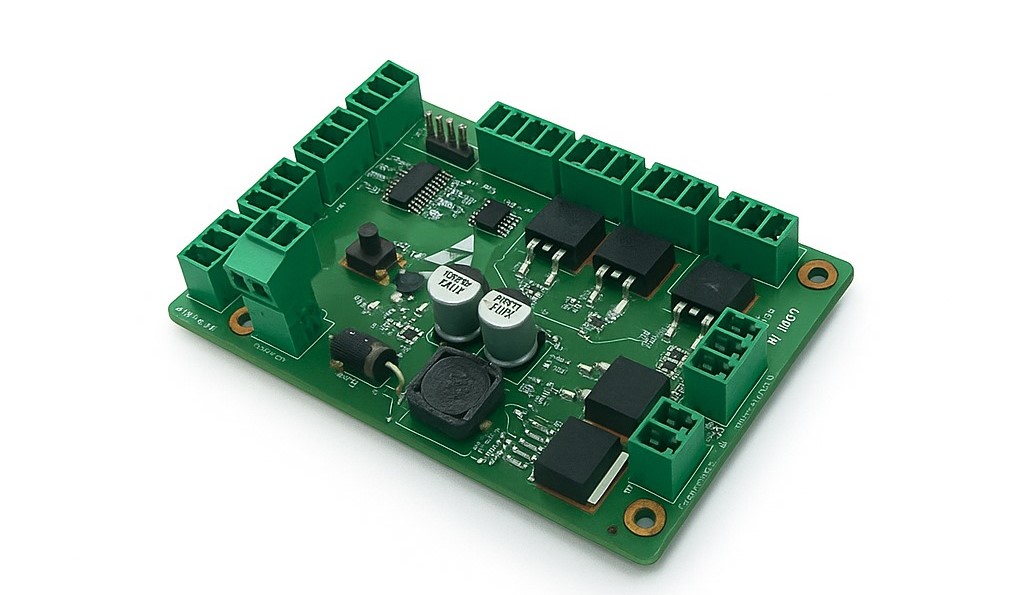
We produce highly precise and reliable control boards for systems that require motor and sensor control, such as filling, labeling, and weighing machines.
Our services go beyond PCB design — we also develop the hardware and embedded software that run on these boards, ensuring a fully integrated system. This allows us to deliver optimized and long-lasting solutions that can be deployed directly on-site.
The PCB design process includes the following stages:
Every project starts with a thorough understanding of the customer’s needs. The intended application, operating voltage, current, board dimensions, and environmental conditions are carefully evaluated.
This analysis forms the foundation of the project, as an industrial PCB must meet different standards and priorities compared to a prototype. Industrial boards emphasize durability, longevity, and safety, while prototypes prioritize flexibility and quick testing.
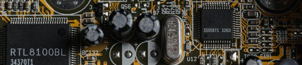
The electronic schematic is created using CAD software. Connections between components such as resistors, capacitors, integrated circuits, and microcontrollers are drawn. This schematic is the heart of the PCB — a single incorrect connection can render the entire board nonfunctional. For this reason, verification and simulation are critical at this stage.
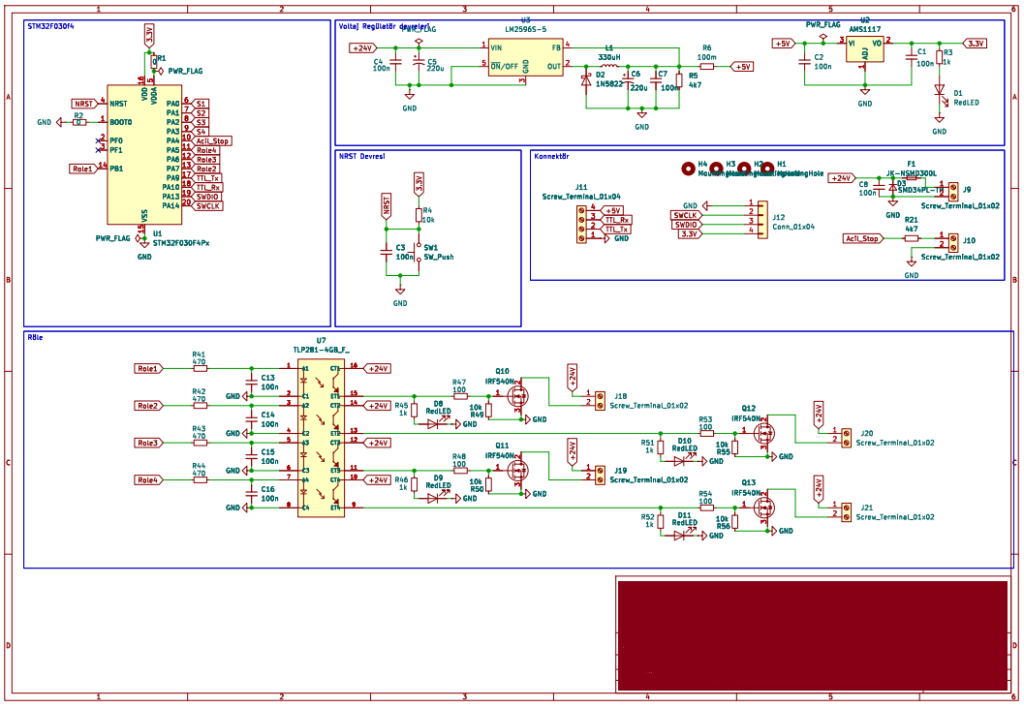
Once the schematic is complete, components are physically placed on the PCB. Factors such as proximity of power components, short signal paths, and the placement of heat-generating parts are carefully considered. A well-designed layout ensures both device stability and ease of manufacturing.
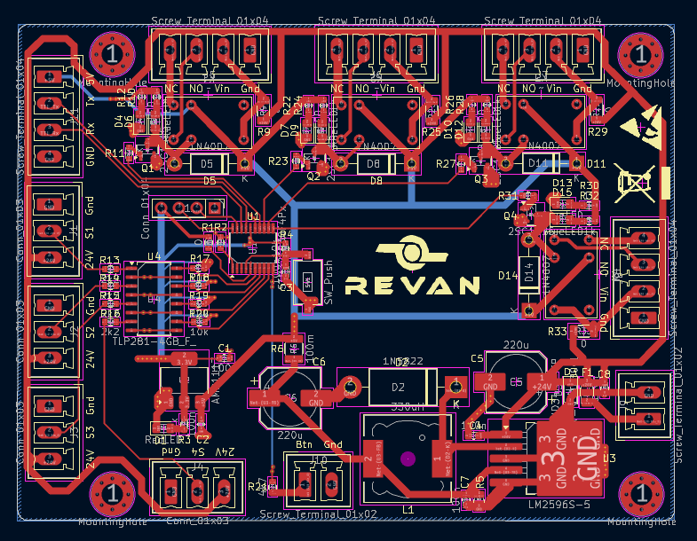
PCBs can be single-layer, double-layer, or multilayer. Compact devices often use multilayer designs to save space. At this stage, signal paths are routed, and broad areas are reserved for power and ground planes. For high-frequency circuits, special design rules must be followed to avoid parasitic effects.
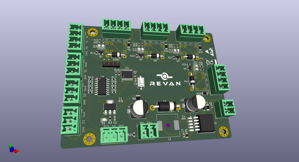
After layout completion, the final board is reviewed in a 3D view. This step ensures the board fits mechanically into its enclosure and that components do not interfere with each other during assembly. The 3D check is crucial for minimizing production errors.
One of the most critical stages in PCB production is the creation of Gerber files — the standard file format understood by PCB manufacturers. These files include information on copper traces, drill holes, silkscreen, and markings. Without Gerber files, no manufacturer can produce your PCB.
The Gerber files are sent to the manufacturer. The production process depends on factors such as material thickness, copper weight, and surface finish. Prototype production can take a few days, while mass production may take several weeks.
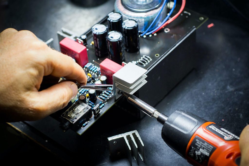
All electronic components are soldered onto the manufactured PCB, either manually or using automated equipment. The circuit is then powered and thoroughly tested to verify correct functionality. This testing phase is essential for ensuring long-term reliability.
A professional PCB design is far more than just a set of drawings. Accurate needs analysis, careful schematic design, proper component placement, and thorough post-production testing all directly impact the quality of the final board. A well-engineered PCB improves device efficiency, minimizes the risk of malfunction, and ensures a long service life.
🔗 Get in touch with us :
Phone/WhatsApp: +41 76 212 8248
✉️ E-Mail: info@revantechnology.com
Discover our recent work:
Revan Technology – Our Projects