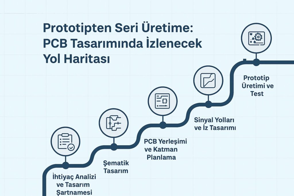
From Prototype to Mass Production: Roadmap for PCB Design
In the realm of electronic product development, the design of Printed Circuit Boards (PCBs) stands as a pivotal phase that directly influences the product’s success. Whether you’re transitioning from a prototype to mass production or embarking on a new project, meticulous planning and execution are paramount. Skipping essential steps can lead to increased manufacturing costs, reduced reliability, and extended time-to-market.
This guide delves into the comprehensive roadmap for PCB design, ensuring a seamless journey from initial concept to large-scale production.
1. Requirements Analysis and Design Specification
The foundation of any successful PCB design lies in a thorough requirements analysis. This phase involves:
- Functional Requirements: Defining the board’s operations, input-output signals, and power needs.
- Physical Requirements: Determining board size, mounting area, and connector placements.
- Environmental Conditions: Assessing factors like temperature, humidity, vibration, and electromagnetic interference (EMI/EMC).
- Standards and Certifications: Ensuring compliance with industry standards such as UL, CE, or RoHS.
A well-prepared design specification serves as a reference throughout the process, minimizing errors during mass production.
2. Schematic Design
Schematic design translates the functional requirements into a logical diagram of the PCB’s electronic circuits. Key considerations include:
- Component Selection: Choosing appropriate microcontrollers, sensors, power regulators, and other components.
- Functional Blocks: Organizing components into power, signal processing, communication, and sensor blocks.
- Connections and Netlists: Defining correct connection points and signal paths for each component.
Circuit simulation tools can be employed to test the schematic design before proceeding to the PCB layout, identifying potential issues early.
3. PCB Layout and Layer Planning
The layout phase determines the physical arrangement of components and the number of layers in the PCB. Important aspects to consider are:
- Layer Count: Simple circuits may use 2 layers; complex or high-speed circuits might require 4 or more layers.
- Ground and Power Planes: Implementing continuous planes is crucial for minimizing EMI and ensuring signal integrity.
- Component Placement: Strategically placing high-frequency components away from noise sources and ensuring critical signal paths are short and direct.
Proper layout planning is essential for optimal PCB performance.
4. Routing and Trace Design
Routing involves creating the electrical paths that connect components on the PCB. Key considerations include:
- Controlled Impedance Traces: Ensuring consistent impedance to prevent signal reflection, especially in high-speed circuits.
- Avoiding Parallel Traces: Minimizing inductive and capacitive interference by not running traces parallel to each other.
- Differential Pairs: Implementing differential pairs for high-speed protocols like USB, Ethernet, or LVDS.
Design Rule Checks (DRC) should be conducted to detect potential errors early in the design process.
5. Thermal Management and EMI/EMC Measures
Effective thermal management and EMI/EMC considerations are vital for PCB reliability. Strategies include:
- Thermal Analysis: Using heatsinks, vias, or thermal pads to dissipate heat from high-power components.
- EMI/EMC Mitigation: Employing ground planes, filters, shielding, and careful component placement to minimize electromagnetic interference.
Simulations can help predict thermal behavior and electromagnetic compatibility before manufacturing.
6. Prototype Production and Testing
Creating PCB prototypes allows for real-world testing and validation. This phase involves:
- Fabrication: Manufacturing the PCB and assembling components using Surface-Mount Technology (SMT) or Through-Hole Technology (THT).
- Functional Tests: Verifying all signal paths, power, and communication functions.
- Debugging and Optimization: Identifying and correcting errors, and revising component placement or routing as needed.
Prototyping is a critical step to ensure the design meets all specifications before mass production.
7. Preparing for Mass Production
Once the prototype is validated, preparations for mass production commence. This includes:
- Gerber Files and Bill of Materials (BOM): Finalizing documentation for manufacturing.
- Production Testing: Utilizing Automatic Test Equipment (ATE) to ensure each board meets quality standards.
- Quality Assurance: Implementing ISO or IPC-compliant quality control measures.
Effective supply chain management, spare parts availability, and logistics planning are also essential for smooth mass production.
8. Continuous Improvement and Documentation
Post-production, it’s crucial to:
- Record Issues: Document any problems encountered during production and provide feedback to the design team.
- Track Changes: Use version control systems to monitor all PCB design modifications.
- Maintain Documentation: Ensure comprehensive documentation is available for technical support and future design revisions.
Continuous improvement practices help in refining designs and processes for future projects.
Conclusion
Transitioning from prototype to mass production in PCB design requires careful planning and execution. By adhering to the outlined roadmap, manufacturers can achieve:
- Enhanced Product Reliability: Through thorough testing and validation.
- Cost Efficiency: By identifying and addressing issues early in the design process.
- Reduced Time-to-Market: Through streamlined design and production processes.
🔗 For more information:
Revantechnology – PCB Solutions