Basics of PCB Design : The Backbone of Modern Electronics
One of the most essential components of any electronic device is the printed circuit board (PCB). It forms the foundation of nearly all the technologies we use daily. From smartphones and computers to cars and medical devices — almost every electronic product contains a PCB. But what exactly is a PCB, how is it designed, and why is it so important? Let’s break it down step by step.
PCB Design
A PCB is a board that holds electronic components in an organized and stable manner.
On an insulating layer — typically made of glass-reinforced FR4 material — copper traces connect the components electrically.
Before PCBs, circuits were connected using wires, which was cumbersome and prone to errors. With the introduction of PCBs, circuits became:
- More reliable
- Neater
- Easier to manufacture
In short, a PCB is the backbone of every electronic circuit.
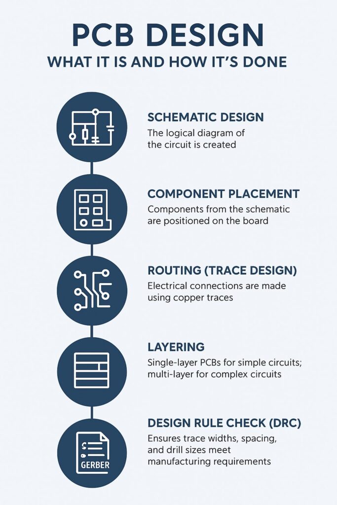
The PCB Design Process
Specialized computer software is used to design PCBs. Popular tools include Altium Designer, KiCad, and Eagle. The design process involves several key steps:
- Schematic Design
The logical circuit is drawn, specifying which component pins connect and how signals flow. - Component Placement
Components defined in the schematic are arranged on the board. Thoughtful placement is crucial for performance.
Examples:- Power supply components in a corner
- Microcontroller in the center
- Connectors along the edges
- Routing
Copper traces establish electrical connections between components. Shorter, organized traces result in a more stable circuit. - Layering
Simple circuits often use a single layer. Complex circuits can use 2, 4, or even 8 layers to save space and reduce electromagnetic interference. - Design Rule Check (DRC)
The design is checked against PCB rules, including trace widths, component spacing, and drill sizes. - Manufacturing Files (Gerber Files)
Once design is complete, Gerber files are generated and sent to the manufacturer to produce the PCB.
Key Considerations in PCB Design
Designing a PCB goes beyond just drawing traces. Important factors include:
- Current Capacity: Traces must be wide enough to handle current without overheating.
- Ground Plane: Large ground areas reduce interference and improve stability.
- Component Placement: Critical parts (like microcontrollers and crystals) should be close together.
- Thermal Management: High-power components require heat dissipation, via copper pours or thermal vias.
- Signal Routing: For high-frequency signals, trace length and parallel placement must be carefully managed.
- Manufacturability: Very fine traces or small pads may cause production errors.
Applications of PCBs
PCBs are used in nearly every sector that relies on electronics:
- Phones and Computers: Motherboards, graphics cards, power circuits
- Automotive: ABS, ECUs, airbags
- Household Appliances: Washing machines, TVs, refrigerators
- Medical Devices: ECG machines, measurement systems, imaging equipment
- Industrial Machines: Automation systems, control panels, robotics
- Defense & Aerospace: Radar, communication systems, flight control
In short, every electrically powered device contains a PCB.
FAQ
Why is a PCB important?
It organizes, stabilizes, and makes electronic circuits manufacturable. Copper traces replace complicated wiring.
How many layers can a PCB have?
Simple PCBs are single-layered. Complex devices can use 2, 4, 6, or more layers to accommodate extensive circuitry.
What materials are most commonly used?
The most common material is FR4. Flexible PCBs use polyimide; high-temperature applications may use ceramic materials.
Conclusion
PCB design directly impacts the performance, durability, and reliability of electronic devices. A well-designed PCB:
- Lasts longer
- Has fewer errors
- Is easier to manufacture
- Operates safely
For electronics beginners, understanding PCBs is essential, as the quality of an electronic product heavily depends on its PCB design.
🔗 Get in touch with us :
Phone/WhatsApp: +41 76 212 8248
✉️ E-Mail: info@revantechnology.com
For detailed information about our services in electronics development & PCB design:
Revan Technology – Your partner for professional electronics and PCB development
Discover our recent work:
Revan Technology – Our Projects